Howdy all,
Bear with me as we talk circuit cards...
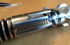
As in Chaim's image, and with feedback in mind, I have widened the traces to 0.1 inches wide, rather than the slightly thinner version I had before. I feel that any other widening of the traces would be in error, due to the foreshortening of the clampcard image, and that the angle it's displayed at is causing us some trouble.

The actual THICKNESS on the board of the plated copper is casting a shadow, as well as causing shadow inside the translucent fiberglass substrate of the card itself. With the lighting in that picture, you can almost see a drop shadow underneath the traces, living kind of inside the card substance beneath the traces. Because of the shadowing effect, I believe trace #1 from the left, had its thin trace actuallt proceed further to the left, and was just severed when the card edge connector section was cut from the main board. You can kind of see the shadow effect of this on that trace, as the cut edge of the board follows a contour consistent with the profile of the layers of copper and metal plating on the traces in comparison to the surface of the fiberglass board material beneath.
As to the vias, I believe there are no square vias ( trace terminations ) on this or any other similar board of this era. I point to these examples:
Note the highlighted traces, as they terminate in small, round circles. Slightly raised, due to the solder flowing into the via, through the board, and to traces on the other side. I believe the lighting of the card in Chaim's images, and due to the fact that we're looking at it from a certain angle, means that the circular shape, and dome of solder is leading us to believe they are more squared.
I am also revising my original opinion that the long wide bars at the top of the clampcard are spacers of some kind, and believe they are just wider traces, similar to the top red highlighted square.
As far as whether or not the vertical traces actually connect to the long horizontal trace, I believe they don't, for the simple reasons that if they did, there wouldn't be a wider via termination circle on the end, and they'd go straight into that horizontal bar. Plenty of examples exist of traces coming VERY close to one another and not touching, and this seems to be the case to me.
As far as the top left corner element, whether or not it's a crescent or what, depends on what it was connected to when the card was cut from the main board. I am at a loss to find an example of such a shape on other similar boards.
Also, a note on whether or not the thin traces originate from the center of the rounded thick traces, remember, these boards were not designed by computer, they were most likely hand drawn, as in this case:
While the thick traces were likely templatized, and standard, the thin ones were most likely drawn in, photoetched, then plated and produced. They might be straight or curved, or whatever the design needed, or the designer felt like drawing.
I welcome any feedback on these thoughts.
Edit:
I also took my layout and perspective matched it to the clamp and card in photoshop, then noticed a few changes that needed to be made.
Here's what I have..
I've updated the image above to match.
")