This is something I've had in mind to do for a while, and only a handful of people were even aware of this project. Now that I've been able to finish up the templates and what not to work from, I felt it was time to post a thread for this:
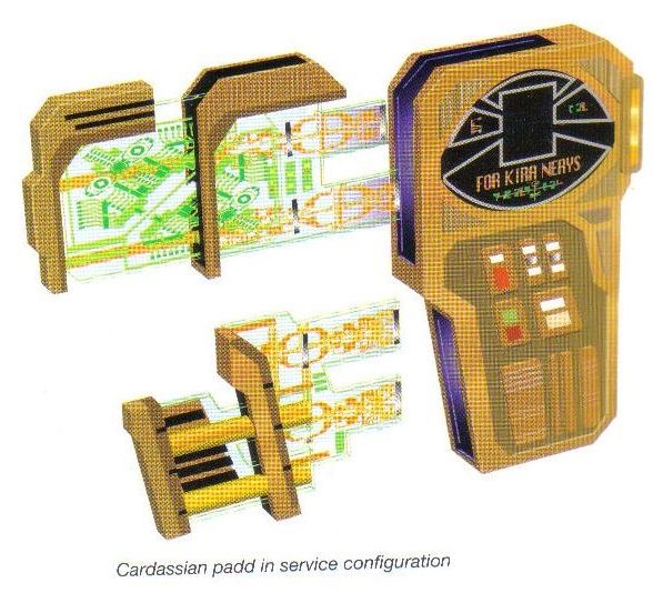
I'd like to thank those who contributed information for both screen-accurate measurements and the close-ups needed to faithfully reproduce the circuitry pattern. Below is a series of pics showing my efforts thus far:
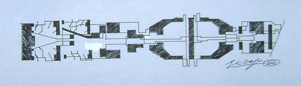
PLANNED CONSTRUCTION OF PADD
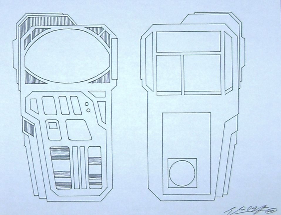
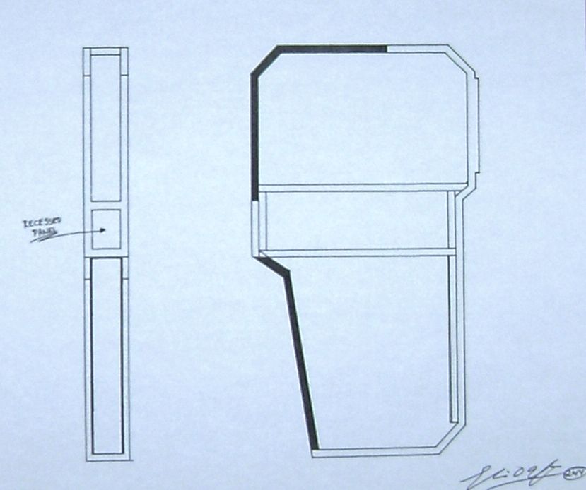
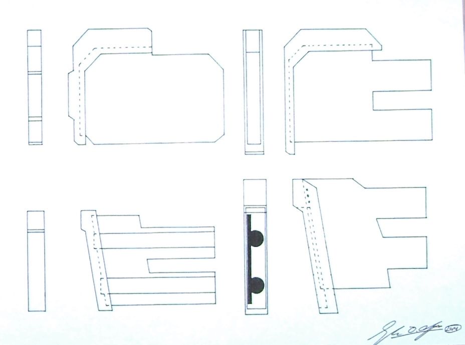
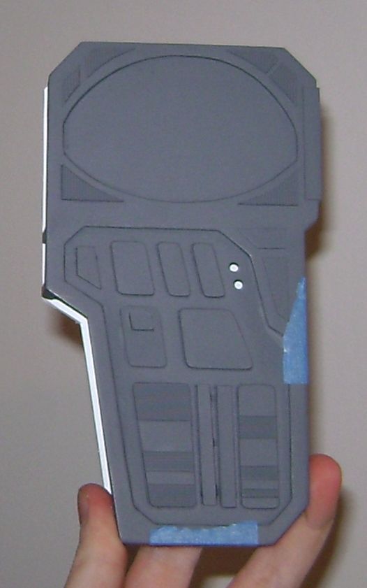
The plan is to make the body out of 1/8" thick sheet styrene, with an internal framework built in to support the four removable circuit boards. The circuit boards themselves will be made of 1/16" thick lexan, with adhesive transparencies applied showing the graphics. As usual, my good pal "ecl" will be the one making the graphics.
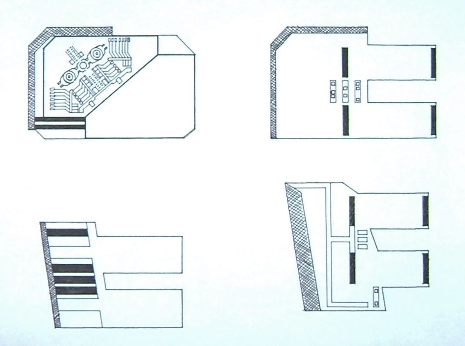
CARDASSIAN CIRCUIT BOARDS LAYOUT
CARDASSIAN CIRCUITRY DETAIL
I tried to reproduce the circuitry detail as faithfully as I could, though the pics I was using had some of the detail obscured. In areas where it was obvious the detail was simply mirrored, I did as such. Other areas I could tell didn't mirror details, though I couldn't make out what those details were supposed to be.
The top-right circuit board will have the circuits applied just as in the pic I've posted above. For the bottom-right one, the circuit will have to be flipped around to match what's seen in the Deep Space Nine Technical Manual exploded view. The black rectangles on both of those will be chrome tape/vinyl on the physical graphics.
For the top-left circuit board, there will be two layers of graphics; the complex circuitry on the front, and two thick orange lines on the back. When the physical graphics are made, each will be on its own adhesive transparency. For the bottom-left one, I think making the brown areas a metallic copper on the physical graphics would really add something to it, given it's the simplest of the four.
Oh, and the circuit pathways for both the green and orange circuit details will be thickened a bit to better match the silk-screening on the screen-used originals. I find what I drew just looks way too thin, but I wanted to be able to clearly differentiate between the various circuit pathways.
Here's where I'm currently at with it, with all of the surface details applied:
I'm now working on the four individual armatures that hold each circuit board.
I also managed to cut out a set of the circuit boards from the 1/16" thick lexan sheet I had left over from my TMP Wrist Comm run:
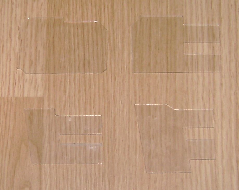
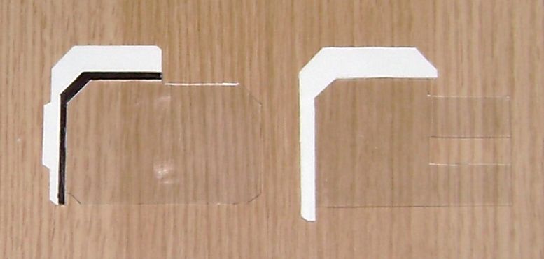
Though I was able to cut out a set of them, I found they took a lot more effort than I'd expected, and they didn't come out looking great. If nothing else, this set will serve as a test bed to ensure everything fits inside as it should.
It may be simpler to see about getting these cut at the plastics shop down the street from where I live.

I'd like to thank those who contributed information for both screen-accurate measurements and the close-ups needed to faithfully reproduce the circuitry pattern. Below is a series of pics showing my efforts thus far:
PLANNED CONSTRUCTION OF PADD


The plan is to make the body out of 1/8" thick sheet styrene, with an internal framework built in to support the four removable circuit boards. The circuit boards themselves will be made of 1/16" thick lexan, with adhesive transparencies applied showing the graphics. As usual, my good pal "ecl" will be the one making the graphics.
CARDASSIAN CIRCUIT BOARDS LAYOUT

CARDASSIAN CIRCUITRY DETAIL

I tried to reproduce the circuitry detail as faithfully as I could, though the pics I was using had some of the detail obscured. In areas where it was obvious the detail was simply mirrored, I did as such. Other areas I could tell didn't mirror details, though I couldn't make out what those details were supposed to be.
The top-right circuit board will have the circuits applied just as in the pic I've posted above. For the bottom-right one, the circuit will have to be flipped around to match what's seen in the Deep Space Nine Technical Manual exploded view. The black rectangles on both of those will be chrome tape/vinyl on the physical graphics.
For the top-left circuit board, there will be two layers of graphics; the complex circuitry on the front, and two thick orange lines on the back. When the physical graphics are made, each will be on its own adhesive transparency. For the bottom-left one, I think making the brown areas a metallic copper on the physical graphics would really add something to it, given it's the simplest of the four.
Oh, and the circuit pathways for both the green and orange circuit details will be thickened a bit to better match the silk-screening on the screen-used originals. I find what I drew just looks way too thin, but I wanted to be able to clearly differentiate between the various circuit pathways.
Here's where I'm currently at with it, with all of the surface details applied:

I'm now working on the four individual armatures that hold each circuit board.
I also managed to cut out a set of the circuit boards from the 1/16" thick lexan sheet I had left over from my TMP Wrist Comm run:


Though I was able to cut out a set of them, I found they took a lot more effort than I'd expected, and they didn't come out looking great. If nothing else, this set will serve as a test bed to ensure everything fits inside as it should.
It may be simpler to see about getting these cut at the plastics shop down the street from where I live.
")


